(China (Mainland))


Product Summary
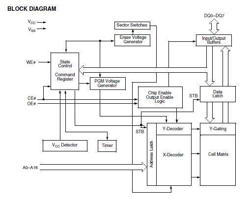
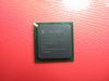
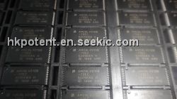
The AM29LV010B-55EI is a 1 Mbit, 3.0 Volt-only Flash memory device organized as 131,072 bytes. The Am29LV010B has a uniform sector architecture. The device is offered in 32-pin PLCC and 32-pin TSOP packages. The byte-wide (x8) data appears on DQ7-DQ0. All read, erase, and program operations are accomplished using only a single power supply. The device can also be programmed in standard EPROM programmers. The AM29LV010B-55EI offers access times of 55, 70, and 90 ns (100 ns part is also available), allowing high speed microprocessors to operate without wait states. To eliminate bus contention, the AM29LV010B-55EI has separate chip enable (CE#), write enable (WE#) and output enable (OE#) controls.
Parametrics
AM29LV010B-55EI absolute maximum ratings: (1)Plastic Packages: -65℃ to +150℃; (2)Ambient Temperature with Power Applied: -65℃ to +125℃; (3)Voltage with Respect to Ground, All pins except A9 and OE#: 0.5 V to VCC+0.5 V; VCC (Note 1): -0.5 V to +4.0 V; (4)A9 and OE# (Note 2): -0.5 V to +12.5 V; (5)Output Short Circuit Current (Note 3): 200 mA.
Features
AM29LV010B-55EI features: (1)Single power supply operation, Full voltage range: 2.7 to 3.6 volt read and write operations for battery-powered application; Regulated voltage range: 3.0 to 3.6 volt read and write operations and for compatibility with high performance 3.3 volt microprocessors; (2)Manufactured on 0.32 μm process technology; (3)High performance, Full voltage range: access times as fast as 55 ns; (4)Ultra low power consumption (typical values at; (5)5 MHz); 200 nA Automatic Sleep mode current; 200 nA standby mode current; 7 mA read current; 15 mA program/erase current; (6)Flexible sector architecture, Eight 16 Kbyte; Supports full chip erase; Sector Protection features; (7)Unlock Bypass Mode Program Command, Reduces overall programming time when issuing multiple program command sequences; (8)Embedded Algorithms, Embedded Erase algorithm automatically preprograms and erases the entire chip or any combination of designated sectors; (9)Embedded Program algorithm automatically writes and verifies data at specified addresses; (10)Minimum 1,000,000 write cycle guarantee per sector; 20 Year data retention at 125℃; Reliable operation for the life of the system; (11)Package option, 32-pin TSOP; 32-pin PLCC; (12)Compatibility with JEDEC standards, Pinout and software compatible with single-power supply Flash; Superior inadvertent write protection; (13)Data# Polling and toggle bits, Provides a software method of detecting program or erase operation completion; (14)Erase Suspend/Erase Resume, Supports reading data from or programming data to a sector that is not being erased.
Diagrams