(China (Mainland))


Product Summary
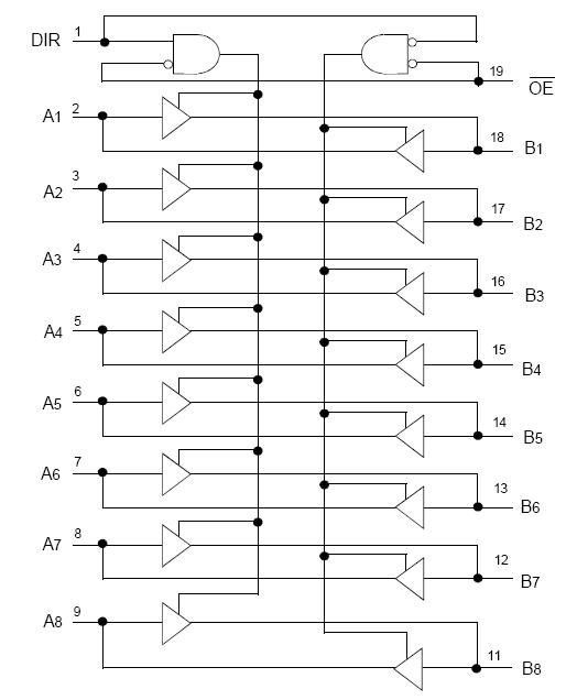
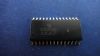
The IDT74LVC245APG50 is a 3.3V CMOS octal bus transceiver with 3-state outputs and 5 volt tolerant I/O. The IDT74LVC245APG50 is ideal for asynchronous communication between two busses (A and B). The direction control pin (DIR) controls the direction of data flow. The output enable pin (OE) overrides the direction control and disables both ports. All inputs are designed with hysteresis for improved noise margin. The applications of the IDT74LVC245APG50 include 5V and 3.3V mixed voltage systems, Data communication and telecommunication systems.
Parametrics
IDT74LVC245APG50 absolute maximum ratings: (1)VIH Input HIGH Voltage Level VCC = 2.3V to 2.7V: 1.7V; (2)VCC = 2.7V to 3.6V: 2V; (3)VIL Input LOW Voltage Level VCC = 2.3V to 2.7V: 0.7V; (4)VCC = 2.7V to 3.6V: 0.8V; (5)IIH Input Leakage Current VCC = 3.6V VI = 0 to 5.5V: ±5μA; (6)IOZH High Impedance Output Current VCC = 3.6V VO = 0 to 5.5V: ±10μA; (7)IOFF Input/Output Power Off Leakage VCC = 0V, VIN or VO≤5.5V: ±50μA; (8)VIK Clamp Diode Voltage VCC = 2.3V, IIN = –18mA: –0.7V; (9)VH Input Hysteresis VCC = 3.3V: 100mV.
Features
IDT74LVC245APG50 features: (1)0.5 MICRON CMOS Technology; (2)ESD>2000V per MIL-STD-883, Method 3015; >200V using machine model (C = 200pF, R = 0); (3)VCC = 3.3V±0.3V, Normal Range; (4)VCC = 2.7V to 3.6V, Extended Range; (5)CMOS power levels (0.4μW typ. static); (6)Rail-to-rail output swing for increased noise margin; (7)All inputs, outputs, and I/O are 5V tolerant; (8)Supports hot insertion; (9)Available in SOIC, SSOP, QSOP, and TSSOP packages.
Diagrams