(China (Mainland))

Product Summary
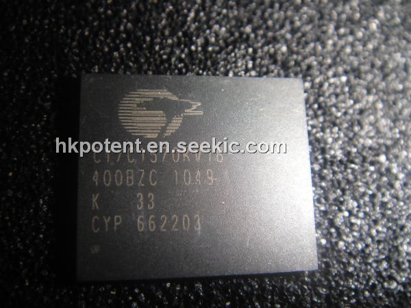
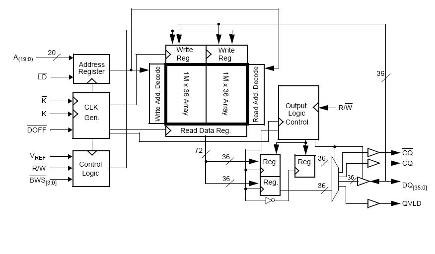
The CY7C1570KV18-400BZC is a 1.8V Synchronous Pipelined SRAM. The CY7C1570KV18-400BZC is equipped with DDR-II+ architecture. The DDR-II+ consists of an SRAM core with advanced synchronous peripheral circuitry. Addresses for read and write are latched on alternate rising edges of the input (K) clock. Write data is registered on the rising edges of both K and K. Read data is driven on the rising edges of K and K. Each address location is associated with two 36-bit words that burst sequentially into or out of the device.
Parametrics
CY7C1570KV18-400BZC absolute maximum ratings: (1)Storage Temperature:–65℃ to +150℃; (2)Ambient Temperature with Power Applied:–55℃ to +125℃; (3)Supply Voltage on VDD Relative to GND:–0.5V to +2.9V; (4)Supply Voltage on VDDQ Relative to GND:–0.5V to +VDD; (5)DC Applied to Outputs in High-Z:–0.5V to VDDQ + 0.3V; (6)DC Input Voltage [12]:–0.5V to VDD + 0.3V; (7)Current into Outputs (LOW): 20mA; (8)Static Discharge Voltage (MIL-STD-883, M 3015): >2001V; (9)Latch-up Current: >200mA.
Features
CY7C1570KV18-400BZC features: (1)72 Mbit density (8M x 8, 8M x 9, 4M x 18, 2M x 36); (2)550 MHz clock for high bandwidth; (3)2-word burst for reducing address bus frequency; (4)Double Data Rate (DDR) interfaces (data transferred at 1100 MHz) at 550 MHz; (5)Available in 2.5 clock cycle latency; (6)Two input clocks (K and K) for precise DDR timing; (7)SRAM uses rising edges only; (8)Echo clocks (CQ and CQ) simplify data capture in high speed systems; (9)Data valid pin (QVLD) to indicate valid data on the output; (10)Synchronous internally self-timed writes; (11)DDR-II+ operates with 2.5 cycle read latency when DOFF is asserted HIGH; (12)Operates similar to DDR-I device with 1 cycle read latency when DOFF is asserted LOW; (13)Core VDD = 1.8V ± 0.1V; IO VDDQ = 1.4V to VDD; (14)Supports both 1.5V and 1.8V IO supply; (15)HSTL inputs and variable drive HSTL output buffers; (16)Available in 165-Ball FBGA package (13 x 15 x 1.4 mm); (17)Offered in both Pb-free and non Pb-free packages; (18)JTAG 1149.1 compatible test access port; (19)Phase-Locked Loop (PLL) for accurate data placement.
Diagrams
| Image | Part No | Mfg | Description |  |
Pricing (USD) |
Quantity | ||||||||||||
|---|---|---|---|---|---|---|---|---|---|---|---|---|---|---|---|---|---|---|
 |
 CY7C1570KV18-400BZC |
Cypress Semiconductor |
SRAM 2Mb x 36 400 MHz |
Data Sheet |
|
|
||||||||||||
| Image | Part No | Mfg | Description | |
Pricing (USD) |
Quantity | ||||||||||||
 |
CY7C006 |
Other |
|
Data Sheet |
Negotiable |
|
||||||||||||
|
CY7C006A |
Other |
|
Data Sheet |
Negotiable |
|
||||||||||||
 |
CY7C006A-15AXC |
Cypress Semiconductor |
SRAM 5V 16Kx8 COM Dual Port SRAM |
Data Sheet |
Negotiable |
|
||||||||||||
|
CY7C006A-15AXCT |
Cypress Semiconductor |
SRAM 5V 16Kx8 COM Dual Port SRAM |
Data Sheet |
Negotiable |
|
||||||||||||
 |
CY7C006A-20AC |
|
IC SRAM 16KX8 DUAL 64LQFP |
Data Sheet |
Negotiable |
|
||||||||||||
|
CY7C006A-20AXC |
Cypress Semiconductor |
SRAM 5V 16Kx8 COM Dual Port SRAM |
Data Sheet |
|
|
||||||||||||