(China (Mainland))

Product Summary
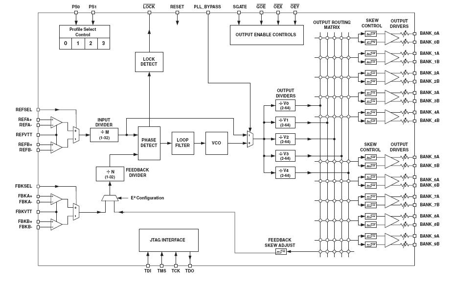
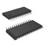
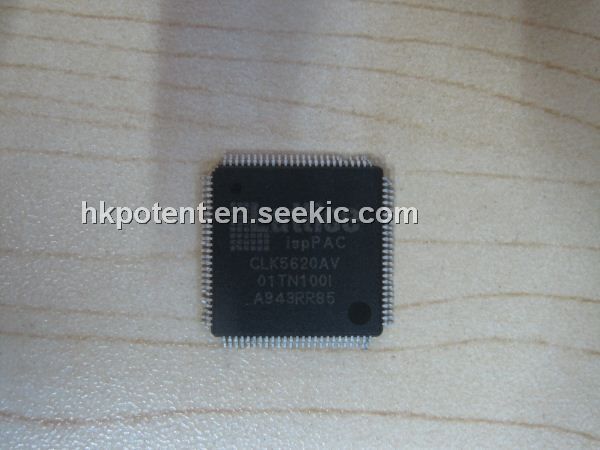
The CLK5620AV-01TN100I is an in-system-programmable high-fanout PLL-based clock driver. The CLK5620AV-01TN100I is designed for use in high performance communications and computing applications. The CLK5620AV-01TN100I provides up to 20 single-ended or 10 differential clock outputs. Each pair of outputs may be independently configured to support separate I/O standards (LVDS, LVPECL, LVTTL, LVCMOS, SSTL, HSTL) and output frequency. In addition, each output provides independent programmable control of termination, slew-rate, and timing skew. All configuration information is stored on-chip in nonvolatile E2CMOS memory.
Parametrics
CLK5620AV-01TN100I absolute maximum ratings: (1)Core Supply Voltage V CCD: -0.5 to 5.5V; (2)PLL Supply Voltage V CCA: -0.5 to 5.5V; (3)JTAG Supply Voltage V CCJ: -0.5 to 5.5V; (4)Output Driver Supply Voltage V CCO: -0.5 to 4.5V; (5)Input Voltage: -0.5 to 4.5V; (6)Output Voltage 1: -0.5 to 4.5V; (7)Storage Temperature: -65 to 150℃; (8)Junction Temperature with power supplied: -40 to 130℃.
Features
CLK5620AV-01TN100I features: (1)10MHz to 320MHz Input/Output Operation; (2)Low Output to Output Skew (<50ps); (3)Low Jitter Peak-to-Peak (<60ps); (4)Up to 20 Programmable Fan-out Buffers; (5)Fully Integrated High-Performance PLL; (6)Precision Programmable Phase Adjustment (Skew) Per Output; (7)Up to Five Clock Frequency Domains; (8)Flexible Clock Reference and External Feedback Inputs; (9)Four User-programmable Profiles Stored in E2CMOS Memory; (10)Full JTAG Boundary Scan Test In-System Programming Support; (11)Exceptional Power Supply Noise Immunity; (12)Commercial (0 to 70℃) and Industrial (-40 to 85℃) Temperature Ranges; (13)100-pin and 48-pin TQFP Packages.
Diagrams