(China (Mainland))

Product Summary
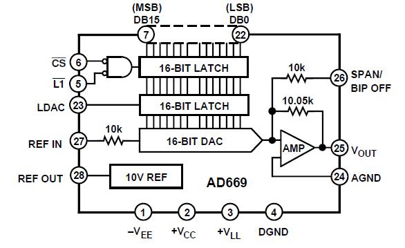
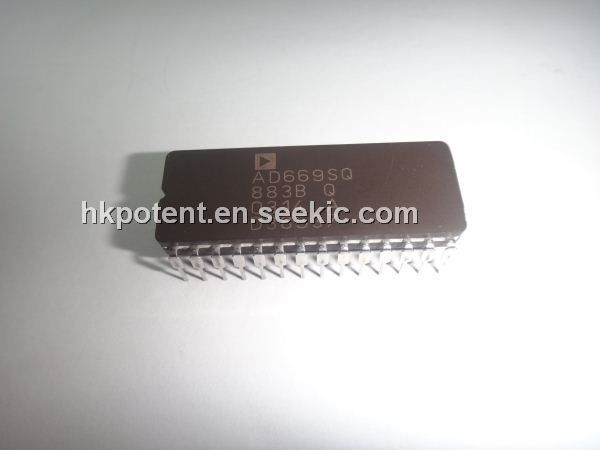
The AD669SQ/883B is a complete 16-bit monolithic D/A converter with an on-board reference and output amplifier. It is manufactured on Analog Devices BiMOS II process. This process allows the fabrication of low power CMOS logic functions on the same chip as high precision bipolar linear circuitry. The AD669SQ/883B chip includes current switches, decoding logic, an output amplifier, a buried Zener reference and double-buffered latches. The AD669SQ/883B’s architecture insures 15-bit monotonicity over temperature. Integral nonlinearity is maintained at ±0.003%, while differential nonlinearity is ±0.003% max.
Parametrics
AD669SQ/883B absolute maximum ratings: (1)VCC to AGND: -0.3 V to +17.0 V; (2)VEE to AGND: +0.3 V to -17.0 V; (3)VLL to DGND: -0.3 V to +7 V; (4)AGND to DGND: ±1 V; (5)Digital Inputs (Pins 5 through 23) to DGND: -1.0 V to +7.0 V; (6)REF IN to AGND: ±10.5 V; (7)Span/Bipolar Offset to AGND: ±10.5 V; (8)REF OUT, VOUT: Indefinite Short To AGND, DGND, VCC, VEE, and VLL; (9)Power Dissipation (Any Package), To +60℃: 1000 mW; (10)Derates above +60℃: 8.7 mW/℃; (11)Storage Temperature: -65℃ to +150℃; (12)Lead Temperature (Soldering, 10 sec): +300℃.
Features
AD669SQ/883B features: (1)Complete 16-Bit D/A Function, On-Chip Output Amplifier; High Stability Buried Zener Reference; (2)Monolithic BiMOS II Construction; (3)61 LSB Integral Linearity Error; (4)15-Bit Monotonic over Temperature; (5)Microprocessor Compatible, 16-Bit Parallel Input; Double-Buffered Latches; (6)Fast 40 ns Write Pulse; (7)Unipolar or Bipolar Output; (8)Low Glitch: 15 nV-s; (9)Low THD+N: 0.009%; (10)MIL-STD-883 Compliant Versions Available.
Diagrams