(China (Mainland))

Product Summary
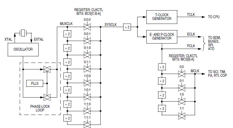
The XC68HC57FN is a microcontroller unit (MCU). The XC68HC57FN is a 16-bit device composed of standard on-chip peripheral modules connected by an intermodule bus. Modules include 16-bit central processor unit (CPU12), Lite integration module (LIM), Two asynchronous serial communications interfaces (SCI0 and SCI1), Serial peripheral interface (SPI), Timer and pulse accumulator module, 8-bit analog-to-digital converter (ATD), 1-Kbyte random-access memory (RAM), 4-Kbyte electrically erasable, programmable read-only memory (EEPROM), Memory expansion logic with chip selects, key wakeup ports, and a phase-locked loop (PLL).
Parametrics
XC68HC57FN absolute maximum ratings: (1)Supply voltage, VDD: -0.3 to +6.5 V; VDDA: -0.3 to +6.5 V; VDDX: -0.3 to +6.5 V; (2)Input voltage, VIn: -0.3 to +6.5 V; (3)Maximum current per pin excluding VDD and VSS, IIn: ± 25 mA; (4)Storage temperature, TSTG: -55 to +150℃; (5)VDD differential voltage, VDD–VDDX: 6.5 V.
Features
XC68HC57FN features: (1)Low-power, high-speed M68HC12 CPU; (2)Power-saving stop and wait modes; (3)Memory: 1024-byte RAM; 4096-byte EEPROM; On-chip memory mapping allows expansion to more than 5-Mbyte address space; (4)Single-wire background debug mode; (5)Non-multiplexed address and data buses; (6)Seven programmable chip-selects with clock stretching (expanded modes); (7)8-channel, enhanced 16-bit timer with programmable prescaler: All channels configurable as input capture or output compare; Flexible choice of clock source; (8)16-bit pulse accumulator; (9)Real-time interrupt circuit; (10)Computer operating properly (COP) watchdog; (11)Clock monitor; (12)Phase-locked loop (PLL); (13)Two enhanced asynchronous non-return-to-zero (NRZ) serial communication interfaces (SCI); (14)Enhanced synchronous serial peripheral interface (SPI); (15)8-channel, 8-bit analog-to-digital converter (ATD); (16)Up to 24 key wakeup lines with interrupt capability; (17)Available in 112-lead low-profile quad flat pack (LQFP) packaging.
Diagrams