(China (Mainland))

Product Summary
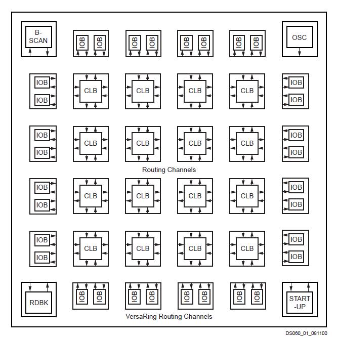
The XC17S30PD8I is a Field Programmable Gate Array implemented with a regular, flexible, programmable architecture of Configurable Logic Blocks (CLBs), interconnected by a powerful hierarchy of versatile routing resources (routing channels), and surrounded by a perimeter of programmable Input/Output Blocks (IOBs), as seen in Figure 1. The XC17S30PD8I has generous
routing resources to accommodate the most complex interconnect patterns. The device is customized by loading configuration data into internal static memory cells. Re-programming is possible an unlimited number of times.
Parametrics
XC17S30PD8I absolute maximum ratings: (1)VCC Supply voltage relative to GND: -0.5 to +7.0 V; (2)VIN Input voltage relative to GND(2,3): -0.5 to VCC +0.5 V; (3)VTS Voltage applied to 3-state output(2,3): -0.5 to VCC +0.5 V; (4)TSTG Storage temperature (ambient): -65 to +150℃; (5)TJ Junction temperature Plastic packages: +125℃.
Features
XC17S30PD8I features: (1)First ASIC replacement FPGA for high-volume production with on-chip RAM; (2)Density up to 1862 logic cells or 40,000 system gates; (3)Streamlined feature set based on XC4000 architecture; (4)System performance beyond 80 MHz; (5)Broad set of AllianceCORE and LogiCORE predefined solutions available; (6)Unlimited reprogrammability; (7)Low cost; (8)System level features, Available in both 5V and 3.3V versions; On-chip SelectRAM memory; Fully PCI compliant; Full readback capability for program verification and internal node observability; Dedicated high-speed carry logic; Internal 3-state bus capability; Eight global low-skew clock or signal networks; IEEE 1149.1-compatible Boundary Scan logic; Low cost plastic packages available in all densities; Footprint compatibility in common packages; (9)Fully supported by powerful Xilinx development system; (10)Foundation Series: Integrated, shrink-wrap software; Alliance Series: Dozens of PC and workstation nthird party development systems supported; Fully automatic mapping, placement and routing.
Diagrams