(China (Mainland))


Product Summary
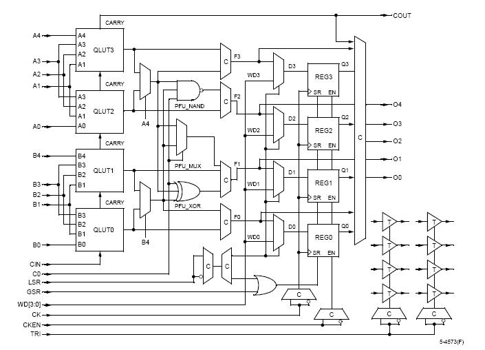
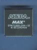
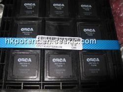
The OR2T40A-5PS208 is a SRAM-based FPGA. It is an enhanced version of the ATT2C/2T architecture. The latest ORCA series includes patented architectural enhancements that make functions faster and easier to design while conserving the use of PLCs and routing resources. The OR2T40A-5PS208 consists of two basic elements: programmable logic cells (PLCs) and programmable input/output cells (PICs). An array of PLCs is surrounded by PICs as shown in Figure 1. Each PLC contains a programmable function unit (PFU). The PLCs and PICs also contain routing resources and configuration RAM. All logic is done in the PFU. Each PFU contains four 16-bit look-up tables (LUTs) and four latches/flip-flops(FFs).
Parametrics
OR2T40A-5PS208 absolute maximum ratings: (1)Storage Temperature Tstg –65 to 150℃; (2)Supply Voltage with Respect to Ground VDD –0.5 to 7.0V; (3)VDD5 Supply Voltage with Respect to Ground (OR2TxxA) VDD5 VDD: 7.0V; (4)Input Signal with Respect to Ground:–0.5 to VDD + 0.3V; (5)Signal Applied to High-impedance Output: –0.5V to VDD + 0.3V; (6)Maximum Soldering Temperature: 260℃.
Features
OR2T40A-5PS208 features: (1)High-performance, cost-effective, low-power; (2)High density; (3)Up to 480 user I/Os; (4)Four 16-bit look-up tables and four latches/flip-flops per PFU, nibble-oriented for implementing 4-, 8-, 16-, and/or 32-bit (or wider) bus structures; (5)Eight 3-state buffers per PFU for on-chip bus structures; (6)Fast, on-chip user SRAM has features to simplify RAM design and increase RAM speed; (7)Improved ability to combine PFUs to create larger RAM structures using write-port enable and 3-state buffers; (8)Fast, dense multipliers can be created with the multiplier mode; (9)Flip-flop/latch options to allow programmable priority of synchronous set/reset vs. clock enable; (10)Enhanced cascadable nibble-wide data path capabilities for adders, subtractors, counters, multipliers, and comparators including internal fast-carry operation.
Diagrams