(China (Mainland))

Product Summary
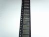
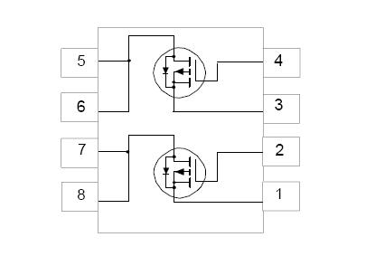
The NDS9953A is a Dual P-Channel Enhancement Mode Field Effect Transistor. The NDS9953A is produced using Fairchild’s proprietary, high cell density, DMOS technology. This very high density process is especially tailored to minimize on-state resistance, provide superior switching performance, and withstand high energy pulses in the avalanche and commutation modes. The NDS9953A is particularly suited for low voltage applications such as notebook computer power management and other battery powered circuits where fast switching, low in-line power loss, and resistance to transients are needed.
Parametrics
NDS9953A absolute maximum ratings: (1)VDSS Drain-Source Voltage: -30V; (2)VGSS Gate-Source Voltage: ±20V; (3)ID Drain Current - Continuous (Note 1a): ±2.9A; (4)Pulsed: ±10A; (5)PD Power Dissipation for Dual Operation: 2W; (6)Power Dissipation for Single Operation (Note 1a): 1.6W; (7)(Note 1b): 1W; (8)(Note 1c): 0.9W; (9)TJ,TSTG Operating and Storage Temperature Range: -55 to 150℃; (10)Thermal Resistance, Junction-to-Ambient (Note 1a): 78℃/W; (11)Thermal Resistance, Junction-to-Case (Note 1): 40℃/W.
Features
NDS9953A features: (1)-2.9A, -30V. RDS (ON) = 0.13W @ VGS = -10V; (2) High density cell design for extremely low RDS (ON); (3) High power and current handling capability in a widely used surface mount package; (4) Dual MOSFET in surface mount package.
Diagrams
| Image | Part No | Mfg | Description |  |
Pricing (USD) |
Quantity | ||||
|---|---|---|---|---|---|---|---|---|---|---|
 |
 NDS9953A |
Fairchild Semiconductor |
MOSFET SO-8 P-CH ENHANCE |
Data Sheet |
Negotiable |
|
||||
|
NDS9953A_D84Z |
Fairchild Semiconductor |
MOSFET |
Data Sheet |
Negotiable |
|
||||