(China (Mainland))

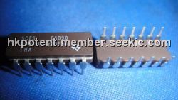
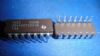
Product Summary
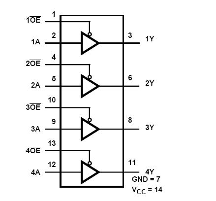
The CD54HCT125F3A is a High-Speed CMOS Logic Quad Buffer. It has its own output enable input, which when “HIGH” puts the output in the high impedance state.
Parametrics
CD54HCT125F3A absolute maximum ratings: (1)DC Supply Voltage, VCC: -0.5V to 7V; (2)DC Input Diode Current, IIK; (3)For VI<-0.5V or VI>VCC + 0.5V: ±20mA; (4)DC Output Diode Current, IOK; (5)For VO<-0.5V or VO>VCC + 0.5V: ±20mA; (6)DC Drain Current, per Output, IO; (7)For -0.5V<VO<VCC + 0.5V: ±35mA; (8)DC Output Source or Sink Current per Output Pin, IO; (9)For VO>-0.5V or VO<VCC + 0.5V: ±25mA; (10)DC VCC or Ground Current, ICC: ±70mA.
Features
CD54HCT125F3A features: (1)Three-State Outputs; (2)Separate Output Enable Inputs; (3)Fanout (Over Temperature Range); (4)Wide Operating Temperature Range: -55℃ to 125℃; (5)Balanced Propagation Delay and Transition Times; (6)Significant Power Reduction Compared to LSTTL Logic ICs; (7)4.5V to 5.5V Operation; (8)Direct LSTTL Input Logic Compatibility, VIL= 0.8V (Max), VIH = 2V (Min); (9)CMOS Input Compatibility, Il≤1μA at VOL, VOH.
Diagrams
 |
 CD54 |
Other |
|
Data Sheet |
Negotiable |
|
||||
|
CD54/74HC161 |
Other |
|
Data Sheet |
Negotiable |
|
||||
|
CD54/74HC163 |
Other |
|
Data Sheet |
Negotiable |
|
||||
|
CD54/74HC192 |
Other |
|
Data Sheet |
Negotiable |
|
||||
|
CD54/74HC193 |
Other |
|
Data Sheet |
Negotiable |
|
||||
|
CD54/74HC240 |
Other |
|
Data Sheet |
Negotiable |
|
||||