(China (Mainland))

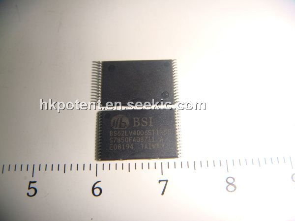
Product Summary
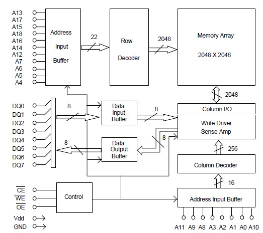
The BS62LV4006STIP55 is a high performance, very low power CMOS Static Random Access Memory. The BS62LV4006STIP55 is organized as 524,288 words by 8 bits and operates from a wide range of 2.4V to 5.5V supply voltage. The BS62LV4006STIP55 technology and circuit techniques provide both high speed and low power features with a typical CMOS standby current of 0.45uA at 3.0V/25℃ and maximum access time of 55ns at 3.0V/85℃. Easy memory expansion is provided by an active LOW chip enable (CE), and active LOW output enable (OE) and three-state output drivers.
Parametrics
BS62LV4006STIP55 absolute maximum ratings: (1)VTERM Terminal Voltage with Respect to GND: -0.5 to Vcc+0.5 V; (2)TBIAS Temperature Under Bias: -40 to +85 ℃; (3)TSTG Storage Temperature: -60 to +150 ℃; (4)PT Power Dissipation: 1.0 W; (5)IOUT DC Output Current: 20mA.
Features
BS62LV4006STIP55 features: (1)Wide Vcc operation voltage : 2.4V ~ 5.5V; (2)Very low power consumption :Vcc = 3.0V C-grade: 29mA (at55ns) operating current; I -grade: 30mA (at55ns) operating current; C-grade: 24mA (at70ns) operating current; I -grade: 25mA (at70ns) operating current; 0.45uA (Typ.) CMOS standby current; (3)Very low power consumption : Vcc = 5.0V C-grade: 68mA (at55ns) operating current; I -grade: 70mA (at55ns) operating current; C-grade: 58mA (at70ns) operating current; I -grade: 60mA (at70ns) operating current; 2.0uA (Typ.) CMOS standby current; (4)High speed access time : 55 55ns; 70 70ns; (5)Automatic power down when chip is deselected; (6)Fully static operation; (7)Data retention supply voltage as low as 1.5V; (8)Easy expansion with CE and OE options; (9)Three state outputs and TTL compatible.
Diagrams