(China (Mainland))

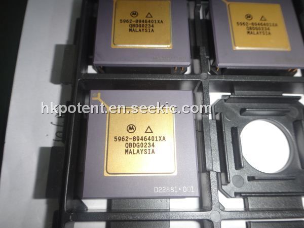

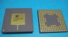
Product Summary
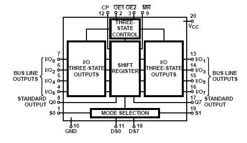
The 5962-8946401XA is an 8-bit shift/storage register with three-state bus interface capability. The 5962-8946401XA has four synchronous-operating modes controlled by the two select inputs as shown in the mode select (S0, S1) table. The mode select, the serial data (DS0, DS7) and the parallel data (I/O0 - I/O7) respond only to the low-to-high transition of the clock (CP) pulse. S0, S1 and data inputs must be stable one setup time prior to the clock positive transition.
Parametrics
5962-8946401XA absolute maximum ratings: (1)DC Supply Voltage, VCC: -0.5V to 7V; (2)DC Input Diode Current, IIK For VI < -0.5V or VI > VCC + 0.5V: ±20mA; (3)DC Output Diode Current, IOK For VO < -0.5V or VO > VCC + 0.5V: ±20mA; (4)DC Drain Current, per Output, IO, For -0.5V < VO < VCC + 0.5V; (5)For Q Outputs: ±25mA; (6)For I/O Outputs: ±35mA; (7)DC Output Source or Sink Current per Output Pin, IO For VO > -0.5V or VO < VCC + 0.5V: ±25mA; (8)DC VCC or Ground Current, ICC: ±50mA.
Features
5962-8946401XA features: (1)Buffered Inputs; (2)Four Operating Modes: Shift Left, Shift Right, Load and Store; (3)Can be Cascaded for N-Bit Word Lengths; (4)I/O0 - I/O7 Bus Drive Capability and Three-State for Bus Oriented Applications; (5)Typical fMAX = 50MHz at VCC = 5V, CL = 15pF, TA = 25℃; (6)Fanout (Over Temperature Range), Standard Outputs: 10 LSTTL Loads; Bus Driver Outputs: 15 LSTTL Loads; (7)Wide Operating Temperature Range: -55℃ to 125℃; (8)Balanced Propagation Delay and Transition Times; (9)Significant Power Reduction Compared to LSTTL Logic ICs; (10)HC Types, 2V to 6V Operation; High Noise Immunity: NIL = 30%, NIH = 30% of VCC at VCC = 5V; (11)HCT Types, 4.5V to 5.5V Operation; Direct LSTTL Input Logic Compatibility, VIL= 0.8V (Max), VIH = 2V (Min); CMOS Input Compatibility, Il . 1μA at VOL, VOH.
Diagrams