(China (Mainland))

Product Summary
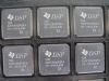
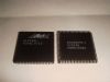
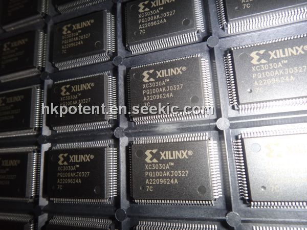
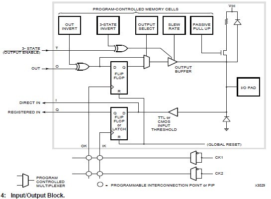
The XC3030A-7PQ100C is a Field Programmable Gate Array (FPGA). The XC3030A-7PQ100C provides a group of high-performance, high-density, digital integrated circuit. Its regular, extendable, flexible, user-programmable array architecture is composed of a configuration program store plus three types of configurable elements: a perimeter of I/O Blocks (IOBs), a core array of Configurable Logic Bocks (CLBs) and resources for interconnection. The development system of the XC3030A-7PQ100C provides schematic capture and auto place-and-route for design entry. Logic and timing simulation, and in-circuit emulation are available as design verification alternatives. The design editor is used for interactive design optimization, and to compile the data pattern that represents the configuration program. The companion the device Configuration PROMs provide a very simple serial configuration program storage in a one-time programmable package. The XC3030A-7PQ100C provides a variety of logic capacities, package styles, temperature ranges and speed grades.
Parametrics
XC3030A-7PQ100C absolute maximum ratings: (1)Supply voltage relative to GND, VCC: -0.5 to +7.0V; (2)Input voltage with respect to GND, VIN: -0.5 to VCC +0.5V; (3)Voltage applied to 3-state output, VTS: -0.5 to VCC +0.5V; (4)Storage temperature (ambient), TSTG: -65 to +150℃; (5)Maximum soldering temperature (10 s @ 1/16 in.), TSOL: +260℃; (6)Junction temperature plastic, TJ: +125℃; (7)Junction temperature ceramic, TJ: +150℃.
Features
XC3030A-7PQ100C features: (1)Complete line of four related Field Programmable Gate Array product families, XC3000A, XC3000L, XC3100A, XC3100L; (2)Ideal for a wide range of custom VLSI design tasks: Replaces TTL, MSI, and other PLD logic; Integrates complete sub-systems into a single package; Avoids the NRE, time delay, and risk of conventional masked gate arrays; (3)High-performance CMOS static memory technology, Guaranteed toggle rates of 70 to 370 MHz, logic delays from 7 to 1.5 ns; System clock speeds over 85 MHz; Low quiescent and active power consumption; (4)Flexible FPGA architecture: Compatible arrays ranging from 1,000 to 7,500 gate complexity; Extensive register, combinatorial, and I/O capabilities; High fan-out signal distribution, low-skew clock nets; Internal 3-state bus capabilities; TTL or CMOS input thresholds; On-chip crystal oscillator amplifier; (5)Unlimited reprogrammability: Easy design iteration; In-system logic changes; (6)Extensive packaging options: Over 20 different packages; Plastic and ceramic surface-mount and pin-gridarray packages; Thin and Very Thin Quad Flat Pack (TQFP and VQFP) options; (7)Ready for volume production: Standard, off-the-shelf product availability; 100% factory pre-tested devices; Excellent reliability record; (8)Complete Development System: Schematic capture, automatic place and route; Logic and timing simulation; Interactive design editor for design optimization; Timing calculator; Interfaces to popular design environments like Viewlogic, Cadence, Mentor Graphics, and others.
Diagrams
| Image | Part No | Mfg | Description |  |
Pricing (USD) |
Quantity | ||||
|---|---|---|---|---|---|---|---|---|---|---|
 |
 XC3030A-7PQ100C |
|
IC LOGIC CL ARRAY 3000GAT 100PQF |
Data Sheet |
Negotiable |
|
||||
| Image | Part No | Mfg | Description | |
Pricing (USD) |
Quantity | ||||
 |
XC3000 |
Other |
|
Data Sheet |
Negotiable |
|
||||
|
XC3000A |
Other |
|
Data Sheet |
Negotiable |
|
||||
|
XC3000L |
Other |
|
Data Sheet |
Negotiable |
|
||||
|
XC3020A-7PC84C |
|
IC LOGIC CL ARRAY 2000GAT 84PLCC |
Data Sheet |
Negotiable |
|
||||
|
XC3030-100PC44C |
|
IC LOGIC CL ARRAY 3000GAT 44PLCC |
Data Sheet |
Negotiable |
|
||||
|
XC3030-100PC68C |
|
IC LOGIC CL ARRAY 3000GAT 68PLCC |
Data Sheet |
Negotiable |
|
||||