(China (Mainland))

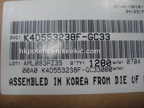
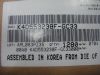
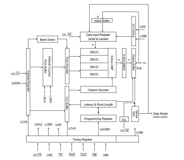
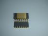
Product Summary
The K4D553238F-GC33 is a 256Mbit GDDR SDRAM. The K4D553238F-GC33 is organized as 4 x 2,097,152 words by 32 bits, fabricated with SAMSUNG’s high performance CMOS technology. Synchronous features with Data Strobe allow extremely high performance up to 2.8GB/s/chip. I/O transactions are possible on both edges of the clock cycle. Range of operating frequencies, programmable burst length and programmable latencies allow the K4D553238F-GC33 to be useful for a variety of high performance memory system applications.
Parametrics
K4D553238F-GC33 absolute maximum ratings: (1)Voltage on any pin relative to Vss VIN, VOUT: -0.5 to 3.6V; (2)Voltage on VDD supply relative to Vss VDD: -1.0 to 3.6V; (3)Voltage on VDD supply relative to Vss VDDQ: -0.5 to 3.6V; (4)Storage temperature TSTG: -55 to +150℃; (5)Power dissipation PD: 3.3W; (6)Short circuit current IOS: 50mA.
Features
K4D553238F-GC33 features: (1)2.5V±5% power supply for device operation; (2)2.5V±5% power supply for I/O interface; (3)SSTL_2 compatible inputs/outputs; (4)4 banks operation; (5)MRS cycle with address key programs; (6)All inputs except data & DM are sampled at the positive going edge of the system clock; (7)Differential clock input; (8)No Wrtie-Interrupted by Read Function; (9)4 DQS’S ( 1DQS / Byte ); (10)Data I/O transactions on both edges of Data strobe; (11)DLL aligns DQ and DQS transitions with Clock transition; (12)Edge aligned data & data strobe output; (13)Center aligned data & data strobe input; (14)DM for write masking only; (15)Auto & Self refresh; (16)32ms refresh period (4K cycle); (17)144-Ball FBGA; (18)Maximum clock frequency up to 350MHz; (19)Maximum data rate up to 700Mbps/pin.
Diagrams