(China (Mainland))

Product Summary
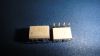
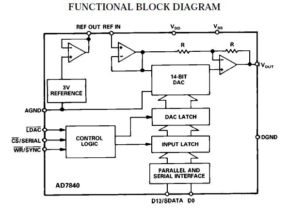
The AD7840JN is a fast, complete 14-bit voltage output D/A converter. The AD7840JN consists of a 14-bit DAC, 3 V buried Zener reference, DAC output amplifier and high speed control logic. The part features double-buffered interface logic with a 14-bit input latch and 14-bit DAC latch. Data is loaded to the input latch in either of two modes, parallel or serial. This data is then transferred to the DAC latch under control of an asynchronous LDAC signal. A fast data setup time of 21 ns allows direct parallel interfacing to digital signal processors and high speed 16-bit microprocessors. In the serial mode, the maximum serial data clock rate can be as high as 6 MHz.
Parametrics
AD7840JN absolute maximum ratings: (1)VDD to AGND: -0.3 V to +7 V; (2)VSS to AGND: +0.3 V to -7 V; (3)AGND to DGND: -0.3 V to VDD + 0.3 V; (4)VOUT to AGND: VSS to VDD; (5)REF OUT to AGND: 0 V to VDD; (6)REF IN to AGND: -0.3 V to VDD + 0.3 V; (7)Digital Inputs to DGND: -0.3 V to VDD + 0.3 V; (8)Operating Temperature Range, Commercial (J, K Versions): 0℃ to +70℃; Industrial (A, B Versions): -25℃ to +85℃; Extended (S Version): -55℃ to +125℃; (9)Storage Temperature Range: -65℃ to +150℃; (10)Lead Temperature (Soldering, 10 sec): +300℃; (11)Power Dissipation (Any Package) to +75℃: 450 mW; (12)Derates above +75℃ by: 10 mW/℃.
Features
AD7840JN features: (1)Complete 14-Bit Voltage Output DAC; (2)Parallel and Serial Interface Capability; (3)80 dB Signal-to-Noise Ratio; (4)Interfaces to High Speed DSP Processors, e.g., ADSP-2100, TMS32010, TMS32020; (5)45 ns min WR Pulse Width; (6)Low Power – 70 mW typ; (7)Operates from 65 V Supplies.
Diagrams
| Image | Part No | Mfg | Description |  |
Pricing (USD) |
Quantity | ||||||||||||||||
|---|---|---|---|---|---|---|---|---|---|---|---|---|---|---|---|---|---|---|---|---|---|---|
 |
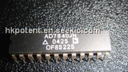
 AD7840JN |
|
IC DAC 14BIT LC2MOS VOUT 24-DIP |
Data Sheet |
|
|
||||||||||||||||
|
AD7840JNZ |
|
IC DAC 14BIT LC2MOS LP 24-DIP |
Data Sheet |
|
|
||||||||||||||||