(China (Mainland))


Product Summary
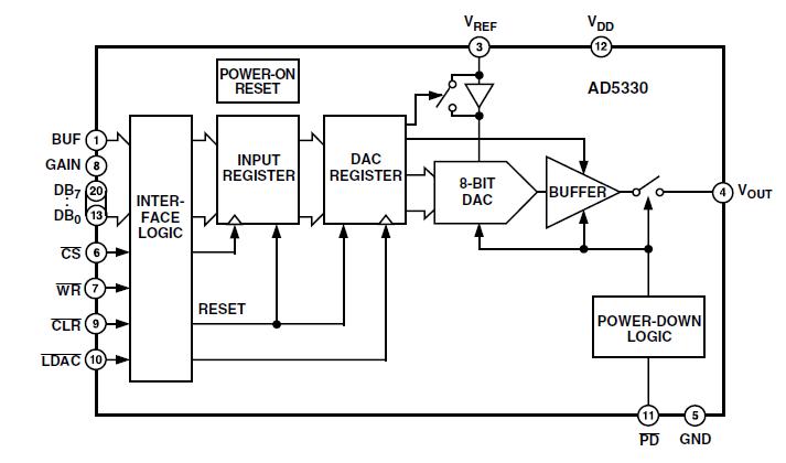
The AD5341BRUZ M is a single 12-bit DAC. The AD5341BRUZ M operates from a 2.5 V to 5.5 V supply consuming just 115 μA at 3 V, and feature a power-down mode that further reduces the current to 80 nA. The device incorporates an on-chip output buffer that can drive the output to both supply rails, while the AD5341BRUZ M allows a choice of buffered or unbuffered reference input. The applications of the AD5341BRUZ M include Portable Battery-Powered Instruments, Digital Gain and Offset Adjustment, Programmable Voltage and Current Sources, Programmable Attenuators, Industrial Process Control.
Parametrics
AD5341BRUZ M absolute maximum ratings: (1)VDD to GND: -0.3 V to +7 V; (2)Digital Input Voltage to GND: -0.3 V to VDD + 0.3 V; (3)Digital Output Voltage to GND: -0.3 V to VDD + 0.3 V; (4)Reference Input Voltage to GND: -0.3 V to VDD + 0.3 V; (5)VOUT to GND: -0.3 V to VDD + 0.3 V; (6)Operating Temperature Range, Industrial (B Version): -40℃ to +105℃; (7)Storage Temperature Range: -65℃ to +150℃; (8)Junction Temperature: 150℃.
Features
AD5341BRUZ M features: (1)AD5341: Single 12-Bit DAC in 20-Lead TSSOP; (2)Low Power Operation: 115 μA @ 3 V, 140 μA @ 5 V; (3)Power-Down to 80 nA @ 3 V, 200 nA @ 5 V via PD Pin; (4)2.5 V to 5.5 V Power Supply; (5)Double-Buffered Input Logic; (6)Guaranteed Monotonic by Design Over All Codes; (7)Buffered/Unbuffered Reference Input Options; (8)Output Range: 0–VREF or 0–2 VREF; (9)Power-On Reset to Zero Volts; (10)Simultaneous Update of DAC Outputs via LDAC Pin; (11)Asynchronous CLR Facility; (12)Low Power Parallel Data Interface; (13)On-Chip Rail-to-Rail Output Buffer Amplifiers; (14)Temperature Range: -40℃ to +105℃.
Diagrams