(China (Mainland))

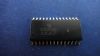
Product Summary
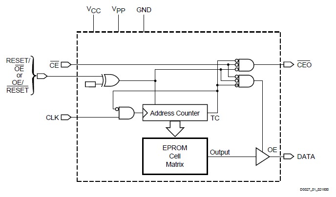
The XC17256E-PD8I is a configuration PROM. It provides an easy-to-use, cost-effective method for storing large Xilinx FPGA configuration bitstreams. When the FPGA is in Master Serial mode, the XC17256E-PD8I generates a configuration clock that drives the PROM. A short access time after the rising clock edge, data appears on the PROM DATA output pin that is connected to the FPGA DIN pin. Once configured, the XC17256E-PD8I disables the PROM. When the FPGA is in Slave Serial mode, the PROM and the FPGA must both be clocked by an incoming signal.
Parametrics
XC17256E-PD8I absolute maximum ratings: (1)VCC Supply voltage relative to GND: –0.5 to +7.0 V; (2)VPP Supply voltage relative to GND: –0.5 to +12.5 V; (3)VIN Input voltage relative to GND: –0.5 to VCC +0.5 V; (4)VTS Voltage applied to High-Z output: –0.5 to VCC +0.5 V; (5)TSTG Storage temperature (ambient): –65 to +150 ℃; (6)TSOL Maximum soldering temperature (10s @ 1/16 in.): +260 ℃.
Features
XC17256E-PD8I features: (1)One-time programmable (OTP) read-only memory designed to store configuration bitstreams of Xilinx FPGA devices; (2)Simple interface to the FPGA; requires only one user I/O pin; (3)Cascadable for storing longer or multiple bitstreams; (4)Programmable reset polarity (active High or active Low) for compatibility with different FPGA solutions; (5)XC17128E/EL, XC17256E/EL, XC1701 and XC1700L series support fast configuration; (6)Low-power CMOS Floating Gate process; (7)XC1700E series are available in 5V and 3.3V versions; (8)XC1700L series are available in 3.3V only.
Diagrams